1366 technologies: a different crystal pulling
1366 Technologies “1366” popped up in the news the other week with its opening of a demonstration plant. Technology Review’s
coverage mainly compared and contrasted its business strategy with that of Solyndra. With only a small bit on the actual technology there is plenty of room for further clarification of it, including determining where 1366’s technology fits into the broader solar landscape. I hate to repeat myself, but it seems useful to go back to the Figures presented in our article on Crystal Solar last year.
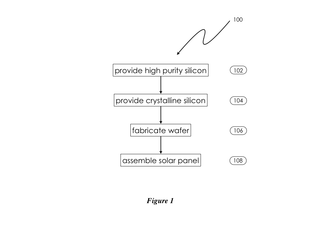
The best place to start is with the flow chart of the most general method of fabricating silicon based solar panels. As shown in Figure 1 method 100 has four broad steps. I think these steps are reasonably self-explanatory. While there is of course further granularity to method 100, everyone has to start with raw silicon and end with a finished panel. The question now is how the method employed by 1366 Technologies fits into method 100.
I guess we first have to determine what they are doing. The Technology page of the 1366 website presents some information on their process, namely
“…is a one-step, kerfless wafer-making process … delivering high quality “drop-in” replacement multicrystalline wafers … directly from molten silicon”.
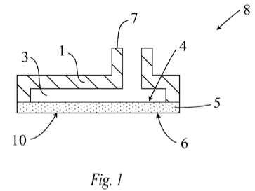
So it appears the 1366 process pulls or fabricates, at least near, net-shape wafers directly from the silicon melt. That is not enough detail though and it is time to see what is filed at the USPTO. Published application US 2011/0247549 “‘549” arose from an assignee search. An assembly that might be used to produce wafers is presented in Figure 1 of ’549 and described in paragraph [0047]. The assembly 8 has a vacuum cavity 3, porous mold sheet 5 and surface 6 (my description). It is disclosed that the assembly 8 may be brought into contact with the surface of molten silicon, and with the surface 6 maintained at a temperature lower than the melting point of Si a sheet of Si solidifies onto it. This sheet is then allowed to grow through the solidification of more silicon onto its surface. Finally, the growing sheet is held to the assembly 8 through the application of a vacuum to cavity 3.
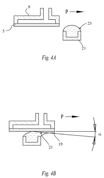
We can now turn to Figures 4A and 4B, which are described in paragraph [0062]. Again we see assembly 8 with mold sheet 5. In this case silicon melt 23 is in trough 21 where it extends over the top thereof. In Figure 4B the assembly 8 is in motion across melt 23. Here thickness 19 of the growing silicon sheet emerges from the melt at interface 21.
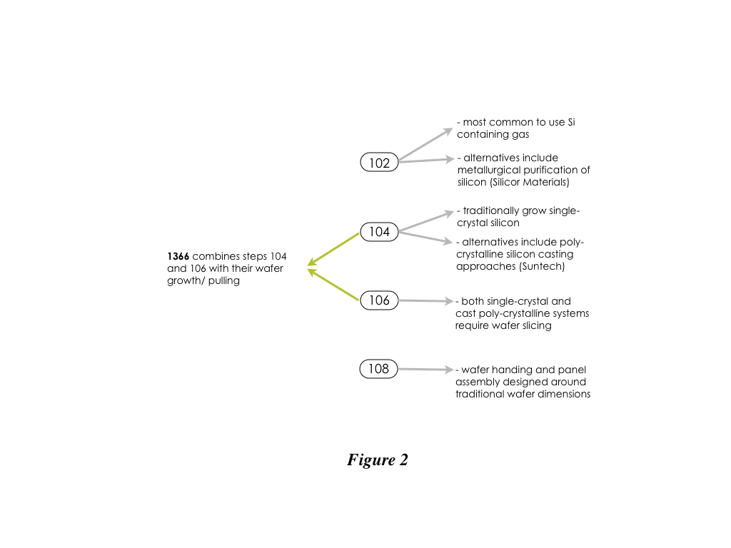
Thus, the apparatus and methods disclosed in ‘549 likely give us an idea of aspects of the wafer forming methods employed by 1366. As we did with Crystal Solar it is instructive to summarize the disclosed method to see how it compares with the the basic process of Figure 1. This is presented in Figure 2. Here we see that 1366 essentially combines steps 104 and 106 into a single wafer forming operation.

